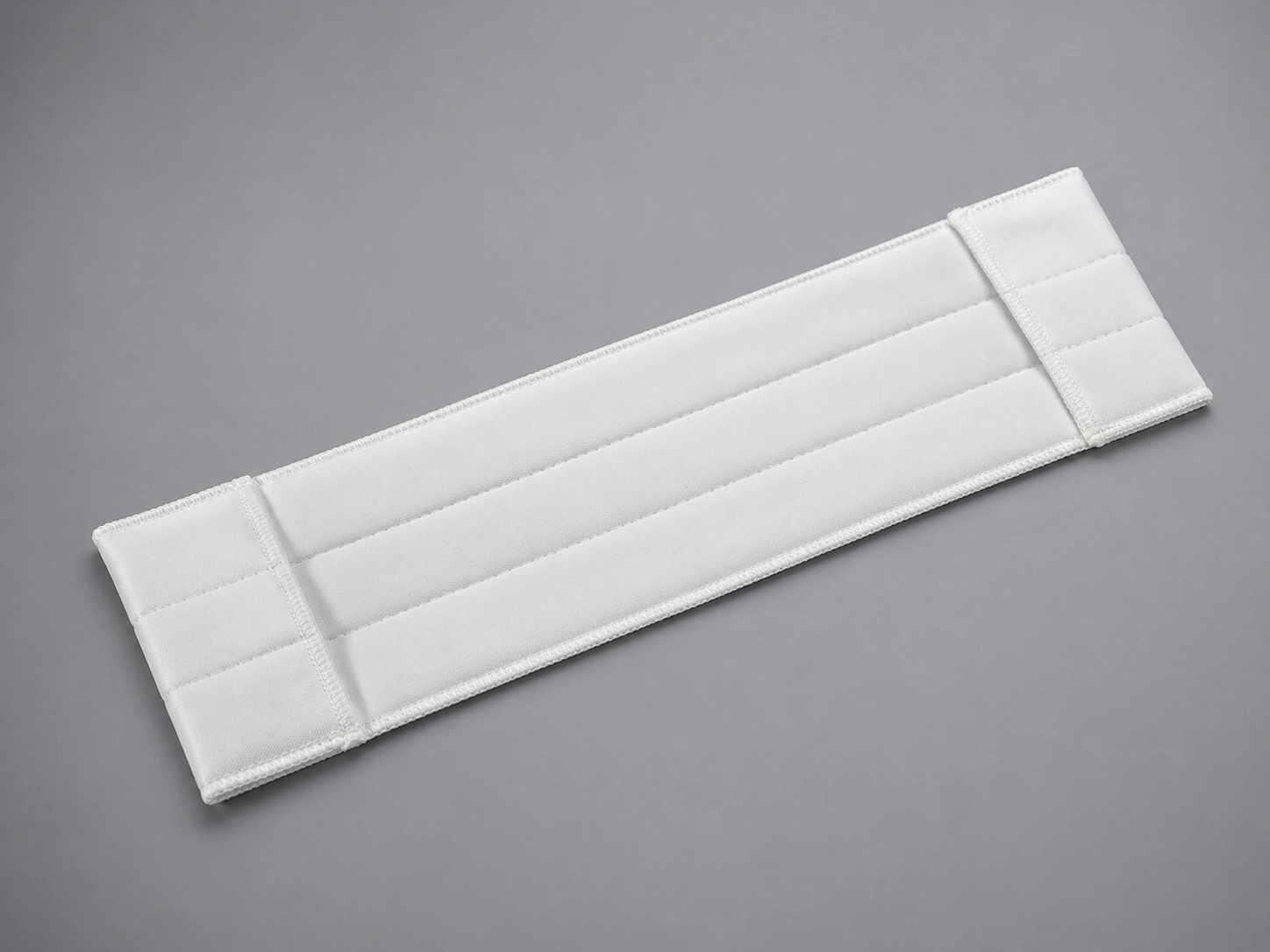
Le nettoyage des salles blanches des semi-conducteurs n’est pas une extension du nettoyage des salles blanches pharmaceutiques. Il impose simultanément trois contraintes qui sont soit absentes, soit dépriorisées dans les contextes pharmaceutiques et biotechnologiques : la sécurité des décharges électrostatiques (ESD), les limites de particules inférieures à 0,1 micron selon la classe ISO 3-5 et la compatibilité avec les solvants de processus agressifs (IPA, acétone, HMDS). Une vadrouille qui fonctionne correctement dans une suite de remplissage pharmaceutique ISO 7 peut introduire des décharges statiques destructrices de plaquettes, dépasser le bilan de particules en suspension dans l'air d'une baie de photolithographie ISO 4 ou se dégrader sous une exposition répétée à l'acétone dans une zone de gravure. Ce guide fournit le cadre de sélection structuré, les exigences zone par zone, la comparaison des spécifications intersectorielles et une liste de contrôle des acheteurs en 8 points dont les installations de semi-conducteurs et les équipes d'approvisionnement ont besoin.

Si une équipe d’approvisionnement s’approvisionne en vadrouilles pour salle blanche en utilisant les mêmes spécifications qu’elles appliquent à une installation pharmaceutique, elle introduira presque certainement un risque de contamination ou d’endommagement du produit dans sa salle blanche de semi-conducteurs. La raison n’est pas qu’une industrie soit plus exigeante que l’autre, mais plutôt que les demandes sont plus grandes. qualitativement différent. Le contrôle de la contamination des salles blanches pharmaceutiques est organisé autour des particules viables (micro-organismes), de l’efficacité du désinfectant et de l’assurance de la stérilité. Le contrôle de la contamination des semi-conducteurs est organisé autour particules non viables, charge électrostatique et intégrité du processus chimique. Les spécifications de la vadrouille doivent refléter cette différence à chaque paramètre.
Le nettoyage des salles blanches des semi-conducteurs diffère du nettoyage des salles blanches pharmaceutiques en trois dimensions fondamentales: (1) Exigences de contrôle ESD qui sont soit absentes, soit facultatives dans le secteur pharmaceutique ; (2) une sensibilité granulométrique jusqu'à 0,1 micron dans les classes ISO 3-5, ce qui est 2 à 4 ordres de grandeur plus stricts que la plage ISO 7-8 typique dans le secteur pharmaceutique ; et (3) l'exposition à des solvants agressifs (IPA, acétone, HMDS, décapants spéciaux) pour lesquels les matériaux de vadrouille de qualité pharmaceutique n'ont peut-être pas été validés. Une spécification de vadrouille qui aborde deux de ces trois dimensions tout en négligeant la troisième n’est pas adaptée à une utilisation en salle blanche pour les semi-conducteurs.
| Dimension de l'exigence | Salle blanche pharmaceutique | Salle blanche pour semi-conducteurs | Implication des spécifications de la vadrouille |
|---|---|---|---|
| Sécurité ESD | Pas généralement requis ; L'ESD est rarement un paramètre de spécification des consommables | Obligatoire dans toutes les zones de manipulation de plaquettes ; résistivité de surface généralement inférieure à 109 Ω/carré | Le matériau de la vadrouille doit incorporer des propriétés antistatiques ou conductrices. Le tricot en polyester standard seul est généralement isolant et peut ne pas répondre aux critères ESD. |
| Bilan de particules en suspension dans l'air | ISO 7 : 352 000 particules/m3 (≥0,5 µm) ; ISO 8 : 3 520 000 particules/m3 (≥0,5 μm) | ISO 4 : 352 particules/m3 (≥0,5 µm) ; ISO 3 : 35 particules/m3 (≥0,5 µm). Le comptage des particules commence à 0,1 μm. | Les limites d’élimination des particules sont 1 000 à 100 000 fois plus strictes. La construction à filament continu et l'étanchéité vérifiée des bords deviennent des exigences opérationnelles et non des recommandations. |
| Exposition chimique | Désinfectants : ammonium quaternaire, peroxyde d'hydrogène, acide peracétique, hypochlorite de sodium | Solvants agressifs : IPA, acétone, HMDS, solution Piranha, décapants photorésistants spéciaux | Les matériaux de vadrouille validés par l'industrie pharmaceutique n'ont peut-être pas été testés contre les solvants. La dégradation chimique du tissu de la vadrouille peut devenir une source cachée de particules que la surveillance environnementale peut ne pas attribuer directement à la vadrouille. |
| Préoccupation de contamination primaire | Particules viables (micro-organismes) + particules non viables. La stérilité est souvent le paramètre dominant. | Les particules non viables constituent la préoccupation dominante. Même les particules invisibles peuvent provoquer des défauts, des courts-circuits ou des ouvertures dans la configuration des plaquettes. | Les tests de perte de particules (tambour Helmke ou équivalent) à la résolution de classe ISO cible ne sont pas négociables. Une allégation « adapté à une utilisation en salle blanche » sans données sur le bac à particules ne constitue pas une preuve. |
Dans une usine de fabrication de plaquettes semi-conductrices, la particule qui compte le plus est invisible. Au niveau du nœud de processus de 3 nm ou de 5 nm, une particule supérieure à la moitié de la dimension critique peut provoquer un défaut mortel : une particule de 1,5 nm peut détruire la structure d'un transistor. Les classifications des salles blanches pour les usines de semi-conducteurs reflètent cette sensibilité : la classe ISO 3 autorise seulement 1 000 particules par mètre cube à des tailles ≥0,1 μm, et la classe ISO 4 autorise 10 000 à ≥0,1 μm. En revanche, la classe ISO 7 – courante dans la fabrication pharmaceutique stérile – autorise 352 000 particules à ≥0,5 μm, et le comptage des particules pour 0,1 μm n’est même pas requis à la norme ISO 7.
L'implication de la vadrouille est directe : chaque contact entre la tête de vadrouille et le sol ou la surface de la salle blanche libère des particules. Une vadrouille qui génère 10 000 particules par mètre carré lors de son utilisation peut être acceptable dans un environnement ISO 7 où le bilan de particules en suspension dans l'air est important. Dans une baie de photolithographie ISO 4, la même vadrouille peut consommer une fraction mesurable du budget total de particules de l’installation par événement de nettoyage. La sélection doit commencer par l’établissement classification ISO la plus stricte, pas avec le classement moyen sur toutes les zones.
Les décharges électrostatiques ne constituent pas un problème de contamination au sens classique du terme : c'est un mécanisme d'endommagement du produit. Une charge statique de quelques centaines de volts, imperceptible pour un opérateur humain, peut détruire une couche d'oxyde de grille mesurée en angströms. La vadrouille est l’un des plus gros objets en mouvement dans la salle blanche qui entre en contact répété et à friction élevée avec les surfaces. La charge triboélectrique générée par le nettoyage – le même mécanisme qui génère de l'électricité statique lorsque les chaussures frottent sur un tapis – peut s'accumuler sur la tête, le cadre et le manche de la vadrouille, puis se décharger dans une tranche ou un support de tranche à proximité.
Les salles blanches pharmaceutiques précisent rarement les exigences ESD pour les outils de nettoyage, car le produit (médicament, produit biologique) n'est pas sensible aux décharges électrostatiques de la même manière. Les usines de semi-conducteurs le doivent. Chaque consommable entrant dans une zone protégée ESD (EPA) doit être classé en fonction de sa résistivité de surface, et les outils de nettoyage ne font pas exception. Les spécifications de la vadrouille doivent concerner non seulement le matériau de la tête de vadrouille, mais aussi l'ensemble de l'ensemble (cadre, manche et tout matériel de fixation), car un seul chemin conducteur dans un outil par ailleurs protégé contre les décharges électrostatiques crée une voie de décharge incontrôlée.
Les désinfectants pharmaceutiques pour salles blanches – composés d’ammonium quaternaire, peroxyde d’hydrogène, acide peracétique, hypochlorite de sodium – sont chimiquement agressifs en eux-mêmes, mais ils sont prévisibles. Les fabricants de consommables pour salles blanches effectuent régulièrement des tests par rapport à des panneaux désinfectants standard. Les solvants du traitement des semi-conducteurs – alcool isopropylique (utilisé pour la déshydratation des surfaces et le nettoyage général), acétone (utilisé pour le décapage des photorésists), HMDS (utilisé pour l’apprêt de la surface des plaquettes) et décapants organiques spécialisés – représentent un défi chimique différent. Ces solvants peuvent extraire les plastifiants, gonfler les fibres synthétiques, dissoudre les revêtements polymères et dégrader les liaisons adhésives dans la construction des vadrouilles – des effets que les programmes de validation des vadrouilles axés sur le secteur pharmaceutique peuvent ne pas couvrir.
L’implication pour l’approvisionnement est simple : l’affirmation d’un fournisseur de vadrouille concernant la « résistance chimique » n’a aucun sens sans précision. quels produits chimiques, à quelle concentration, pour quelle durée de contact et avec quel effet mesuré. Les données de compatibilité spécifiques aux solvants doivent faire partie de l’évaluation du fournisseur. Si cette information n'est pas disponible, l'installation doit soit procéder à sa propre évaluation de compatibilité, soit exclure le fournisseur de la prise en compte des zones où une exposition aux solvants est attendue.
La sélection des matériaux de vadrouille antistatique commence par la compréhension des classifications de résistivité de surface définies par les normes industrielles. ANSI/ESD S20.20 et CEI 61340-5-1 établissent le cadre de classification des matériaux dans les zones protégées ESD, et les vadrouilles pour salles blanches entrent dans ce cadre en tant que consommables mobiles générant des frictions.
| Classification | Plage de résistivité de surface (Ω/carré) | Comportement de charge | Pertinence pour la vadrouille en salle blanche |
|---|---|---|---|
| Conducteur | < dix4 | La charge circule librement – chemin de décharge rapide | Rarement requis pour les têtes de vadrouille. Plus pertinent pour les surfaces de travail et les revêtements de sol. Une tête de vadrouille conductrice dans une EPA sans chemin de mise à la terre contrôlé peut créer un scénario de décharge dangereux. |
| Dissipatif statique (gamme basse) | dix4 – 107 | La charge se dissipe de manière contrôlée et à vitesse modérée | Convient aux zones de photolithographie ISO 3-4 où le contrôle des particules et la sensibilité ESD sont extrêmes. Peut nécessiter une intégration de fibres conductrices spécialisées. |
| Dissipatif statique (gamme haute) | dix7 – 109 | La charge se dissipe de manière contrôlée et plus lente | Exigence la plus courante en matière de consommables pour vadrouilles à semi-conducteurs pour salles blanches. Réalisable grâce à l'intégration de fils de carbone ou au traitement de surface dissipateur d'électricité statique du tissu en polyester. |
| Antistatique (faible charge) | dix9 – 1011 | Résiste à la génération de charges triboélectriques mais ne se dissipe pas rapidement | Peut être acceptable pour les zones d'emballage/back-end ISO 6-7 où la sensibilité ESD est plus faible et où la principale préoccupation est la génération de charges pendant le nettoyage plutôt que la dissipation des charges existantes. |
| Isolant | > dix11 | La charge s'accumule ; pas de chemin de dissipation contrôlé | Ne convient généralement pas aux zones sensibles aux ESD. Le tricot standard 100 % polyester et la microfibre non traitée entrent généralement dans cette gamme. Ces matériaux sont courants dans les salles blanches pharmaceutiques mais ne doivent pas être déployés dans les EPA de semi-conducteurs sans vérification ni traitement. |
Il existe deux approches principales pour rendre les matériaux de vadrouille pour salle blanche sûrs ESD :
Le choix entre ces approches dépend du modèle d’utilisation de la vadrouille de l’installation (jetable ou réutilisable), de la plage de résistivité cible et du profil d’exposition chimique de la zone. Pour les vadrouilles jetables en photolithographie ISO 3-4, l’une ou l’autre approche peut convenir à condition que les données de résistivité soient vérifiées. Pour les vadrouilles réutilisables exposées à des solvants agressifs, l'intégration de fils de carbone offre généralement des performances ESD à long terme plus constantes que les traitements de surface. Pour une discussion plus large sur les produits de vadrouille spécifiques aux semi-conducteurs, voir produits de vadrouille pour salle blanche à semi-conducteurs.
La sécurité ESD est une propriété du système et non une propriété des composants. Une tête de vadrouille avec une résistivité de surface de 108 Ω/carré n'offre aucune protection ESD si les vêtements de l'opérateur, le sol de la salle blanche et l'ensemble cadre/poignée de vadrouille n'effectuent pas un chemin de dissipation contrôlé vers la terre. La vadrouille est un maillon de la chaîne de mise à la terre :
Les installations doivent vérifier la compatibilité ESD pour l’ensemble complet (tête de vadrouille, cadre, manche, EPI de l’opérateur et revêtement de sol) plutôt que de spécifier les exigences ESD pour la tête de vadrouille isolément. Une vadrouille pour salle blanche qui répond aux spécifications de résistivité ESD lors d'une mesure en laboratoire peut ne pas fonctionner comme un outil sécurisé ESD dans la salle blanche réelle si le chemin de dissipation au niveau de l'assemblage est incomplet.
La génération de particules à partir d’une vadrouille pour salle blanche n’est pas une propriété réussite/échec : il s’agit d’une mesure quantitative qui doit être évaluée par rapport au bilan de particules en suspension dans l’air de la classe ISO cible. Une vadrouille qui génère 5 000 particules par minute dans un tambour Helmke peut être excellente pour la norme ISO 7 mais inacceptable pour la norme ISO 4, où le nombre total de particules ≥0,5 μm autorisé n'est que de 352 par mètre cube. Les spécifications de la vadrouille doivent correspondre à la zone la plus stricte dans laquelle la vadrouille sera utilisée.
Le choix de matériau fondamental affectant la génération de particules est la construction des fibres :
| Type de fibre | Construction | Mécanisme de génération de particules | Aptitude typique |
|---|---|---|---|
| Polyester à filaments continus | Des filaments longs et ininterrompus s'étendent sur toute la longueur du fil. Aucune fibre ne se termine dans la structure du tissu, sauf au niveau des bords coupés. | Les particules sont principalement générées au niveau des bords coupés (qui doivent être scellés) et par l'abrasion de la surface. La perte des extrémités des fibres dans le corps du tissu est intrinsèquement faible car il n'y a pas d'extrémités de fibres discontinues pouvant se libérer. | Fortement préféré pour les zones semi-conductrices ISO 3-5. Le profil de perte de particules intrinsèquement plus faible fait du filament continu le point de départ par défaut pour la sélection d'une vadrouille inférieure à la norme ISO-5. |
| Polyester à fibres discontinues/non continues | Les fibres courtes (généralement de 25 à 50 mm) sont filées ensemble pour former du fil. Des milliers d’extrémités de fibres existent dans la structure du tissu. | Les fibres discontinues individuelles peuvent se séparer du fil lors de l'agitation mécanique (vadrouille). Chaque extrémité de la fibre est une particule potentielle qui peut se détacher. Le nombre de particules provenant des constructions en fibres discontinues est généralement plus élevé que celui des filaments continus pour les mêmes conditions de test. | Peut être évalué pour les zones ISO 6-7. Généralement non recommandé pour les normes ISO 3-5 sans les données du tambour Helmke démontrant une élimination acceptable des particules à la taille et à la classe de particules cibles. |
| Microfibre (polyester fendu/polyamide) | Les fibres bi-composantes sont divisées en filaments micro-deniers (généralement <1 denier par filament). La structure divisée crée une surface élevée pour la capture des particules. | La même surface élevée qui confère à la microfibre son efficacité de capture des particules crée également plus de surface à partir de laquelle les particules peuvent se détacher. Les pointes en fibres fendues sont des sources potentielles de particules. Le composant polyamide (nylon) ajoute un deuxième matériau avec ses propres caractéristiques d'élimination des particules et de compatibilité chimique. | Peut être évalué pour les zones semi-conductrices ISO 5-7. Nécessite une vérification plus rigoureuse de la perte de particules pour ISO 3-4 que le polyester à filament continu. Le compromis efficacité de nettoyage/élimination des particules doit être évalué zone par zone. |
L'image du corps ci-dessous illustre la structure des fibres de polyester à filament continu — la surface lisse et non pelucheuse sans extrémités de fibres discontinues lâches qui rend cette construction préférable pour les têtes de vadrouille pour salles blanches à faible génération de particules dans les environnements semi-conducteurs.
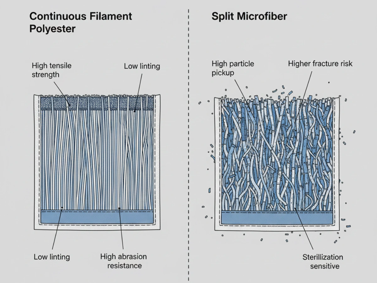
Pour une évaluation côte à côte de la microfibre et du polyester dans les applications en salle blanche, voir le Comparaison des vadrouilles en microfibre et en polyester pour salle blanche.
Que le tissu soit à filament continu ou non continu, le les bords coupés sont la source de particules la plus concentrée sur n’importe quelle tête de vadrouille pour salle blanche. Lorsque le tissu est coupé, les filaments sont sectionnés, créant des extrémités de fibres qui peuvent libérer des particules à chaque agitation mécanique. La qualité du scellement des bords détermine l’efficacité avec laquelle ces particules de pointe sont contenues :
Les équipes d'approvisionnement doivent demander des informations sur la méthode de scellement des bords et vérifier que les quatre bords de la tête de balai sont scellés, et pas seulement les bords visibles. Pour une compréhension plus approfondie du lien entre la génération de peluches et la construction d'une vadrouille, voir qu'est-ce qu'une vadrouille pour salle blanche peu pelucheuse.
Le test au tambour Helmke (selon IEST-RP-CC004.3 ou équivalent) est la méthode standard pour quantifier la perte de particules provenant des consommables de salle blanche sous agitation mécanique. Pour l’évaluation d’une vadrouille de qualité semi-conducteur, les paramètres de test et attentes suivants s’appliquent :
Distinction critique : La norme ISO 14644 classe environnements, pas produits. Un fournisseur affirmant qu'une vadrouille est « compatible ISO classe 5 » sans fournir la méthode de test, les compartiments de granulométrie, les valeurs mesurées et les conditions de test fait une affirmation invérifiable. Les équipes des établissements doivent traiter ces allégations comme un langage marketing et non comme une preuve technique, jusqu'à ce que les données de test soient fournies.
L’environnement chimique dans une usine de fabrication de semi-conducteurs présente des problèmes de compatibilité des matériaux de vadrouille que les guides de sélection de vadrouilles pour salles blanches pharmaceutiques ne traitent pas. Un matériau de vadrouille pour salle blanche qui résiste à une exposition répétée aux désinfectants à base d'ammonium quaternaire peut se dégrader rapidement au contact de l'acétone. Le processus d’approvisionnement doit vérifier la compatibilité avec le panel chimique spécifique de l’installation – et non avec une allégation générique de « résistance aux produits chimiques ».
L'alcool isopropylique (IPA) à une concentration de 70 à 99 % est le solvant de nettoyage le plus courant dans les salles blanches pour semi-conducteurs. Il est utilisé pour la déshydratation des surfaces, l’essuyage général et l’élimination des résidus organiques. Bien que l'IPA soit moins agressif que l'acétone ou le HMDS, c'est un pénétrant qui peut extraire les plastifiants des matériaux polymères, gonfler certaines fibres synthétiques et dégrader les liaisons adhésives utilisées dans la construction des vadrouilles.
Pour les matériaux de vadrouille à base de polyester, la compatibilité IPA est généralement bonne : le polyester (PET) possède une résistance inhérente aux solvants à base d'alcool. Toutefois, les éléments suivants nécessitent une vérification :
L'acétone est utilisée dans les usines de fabrication de semi-conducteurs pour l'élimination des photorésists, le nettoyage des équipements et le dégraissage général. C'est un solvant organique puissant qui attaque une gamme de polymères plus large que l'IPA :
| Agent chimique | Utilisation courante des semi-conducteurs | Compatibilité avec les matériaux de vadrouille | Vérification requise |
|---|---|---|---|
| IPA (70-99%) | Nettoyage général des surfaces, déshydratation, pré-essuyage pour équipements de process | Polyester : Généralement bon. Polyamide : Passable à médiocre — gonflement possible. Traitements ESD : Peut se dégrader. | Évaluation de l'excrétion de particules après exposition. Re-mesure de la résistivité ESD après contact IPA pour les vadrouilles réutilisables. |
| Acétone | Décapage de photorésist, élimination de résidus organiques lourds, dégraissage d'équipements | Polyester : Peut tolérer un bref contact ; une exposition prolongée peut provoquer un gonflement et une perte de résistance à la traction. Polyamide : Médiocre – dégradation importante attendue. Adhésifs : La plupart des adhésifs standards échouent sous l’exposition à l’acétone. | Test d'immersion par contact prolongé. Changement de poids, changement de résistance à la traction et inspection visuelle de la dégradation du matériau après exposition à l'acétone à une concentration et une durée adaptées à l'installation. |
| HMDS | Apprêt de surface de plaquette pour l'adhésion de résine photosensible | Réagit avec l'humidité. Peut ne pas attaquer directement les matériaux de la vadrouille mais peut déposer des résidus qui altèrent les performances de nettoyage ultérieur. | Analyse des résidus après contact simulé. Caractérisation de la surface du matériau de vadrouille après exposition au HMDS. |
| Solution Piranha (H2DONC4 +H2Ô2) | Nettoyage agressif des équipements, élimination des résidus organiques | Hautement oxydant – attaque la plupart des polymères organiques, y compris le polyester. Le contact de la vadrouille avec la solution Piranha doit généralement être évité à moins que le matériau de la vadrouille n'ait été spécifiquement validé pour cette exposition. | Si le contact de la vadrouille avec Piranha est inévitable, demandez des données de compatibilité spécifiques au matériau à la concentration et à la température exactes de l’installation. La plupart des matériaux de vadrouille standard pour salles blanches se dégraderont sous l’exposition au Piranha. |
La dégradation chimique des matériaux des vadrouilles constitue un risque de contamination que les programmes de surveillance environnementale peuvent ne pas attribuer directement à la vadrouille, car l'effet est graduel et cumulatif. Le mécanisme fonctionne comme suit :
Cette chaîne de dégradation montre pourquoi les données de compatibilité spécifiques aux solvants ne sont pas une nécessité mais une exigence opérationnelle. Un matériau de vadrouille qui se dégrade selon le profil d’exposition chimique de l’installation génère une contamination difficile à isoler, à diagnostiquer et à éliminer après coup.
Spécifier une vadrouille de salle blanche pour l’ensemble d’une usine de semi-conducteurs est une simplification des achats qui crée un risque de contamination. Différentes zones de fabrication ont différentes classifications ISO, différents niveaux de sensibilité ESD, différents profils d'exposition aux produits chimiques et différentes fréquences de nettoyage. Les spécifications de la vadrouille doivent refléter les exigences de chaque zone – ou, si une seule spécification est utilisée pour l’efficacité des achats, elle doit être validée par rapport aux exigences de la zone la plus stricte, étant entendu que cela peut entraîner des spécifications excessives pour les zones moins exigeantes.
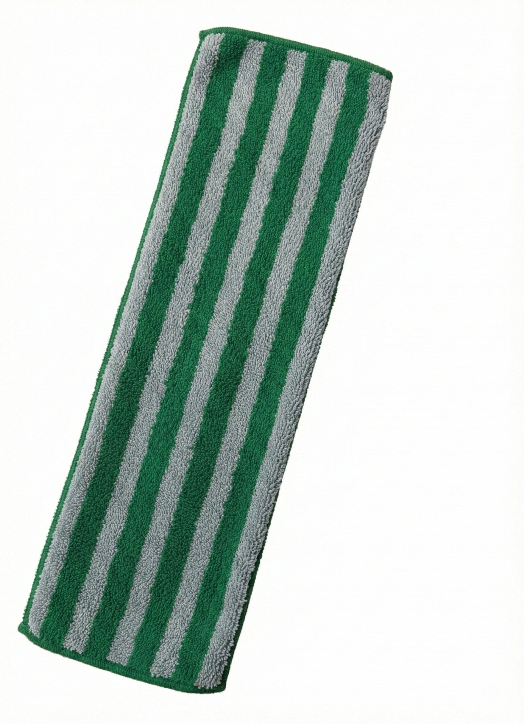
L'ensemble complet du système de vadrouille (tête de vadrouille, cadre en acier inoxydable et manche télescopique) est présenté ci-dessous sous la forme d'une plate-forme de nettoyage intégrée adaptée aux environnements de salle blanche de semi-conducteurs et d'électronique où la compatibilité au niveau du système est essentielle au contrôle de la contamination.
Les baies de photolithographie représentent l'intersection des limites de particules les plus strictes et de la sensibilité ESD la plus élevée dans n'importe quelle usine de semi-conducteurs. Les particules générées lors du nettoyage dans une zone de photolithographie peuvent se déposer sur un photomasque ou sur la surface d'une tranche, créant un défaut de motif qui rend la tranche inutilisable. Le photomasque lui-même est un composant à point de défaillance unique : un défaut de particule sur un masque est répliqué sur chaque tranche exposée à travers ce masque.
Spécifications du balai pour la photolithographie :
Les zones de gravure et de polissage chimico-mécanique (CMP) combinent une sensibilité modérée aux particules avec l'environnement chimique le plus agressif de l'usine. Les processus de gravure utilisent des acides et des bases forts qui peuvent se répandre ou se vaporiser sur les sols et les surfaces des équipements. La boue CMP contient des particules abrasives qui, combinées à des produits chimiques de nettoyage, créent un environnement de nettoyage chimiquement et mécaniquement agressif.
Spécifications du balai pour gravure/CMP :
Les zones de métrologie abritent des équipements de mesure et d’inspection – microscopes électroniques à balayage (MEB), microscopes à force atomique (AFM), outils d’inspection optique – où une seule particule en suspension dans l’air peut interférer avec la précision des mesures. Les limites de particules sont aussi strictes que pour la photolithographie, mais les exigences ESD peuvent être spécifiques à l'équipement plutôt qu'à l'ensemble de la zone.
Spécifications du balai pour la métrologie :
Les zones d'emballage et d'assemblage final fonctionnent selon des classifications de particules moins strictes, mais gèrent des dispositifs finis ou presque finis où les dommages ESD ont un impact sur le rendement. Le débit est plus élevé que dans les zones frontales : la fréquence de nettoyage peut être plus élevée et le taux de consommation de consommables de vadrouille est en conséquence plus élevé.
Spécifications de la vadrouille pour l'emballage/l'assemblage :
Pour plus d'informations sur les exigences de nettoyage spécifiques aux installations de semi-conducteurs, consultez le vadrouille pour salle blanche pour installation de semi-conducteurs page.
La différence entre un fournisseur crédible de vadrouilles pour salles blanches et un fournisseur faisant des allégations invérifiables réside dans la documentation. Les équipes d'approvisionnement en semi-conducteurs doivent demander la documentation suivante dans le cadre du processus d'évaluation des fournisseurs. Chaque élément doit être étayé par des données de test, et non par une assurance verbale ou des déclarations marketing.
Le dégazage (la libération de composés volatils par des matériaux sous vide ou à température élevée) est une préoccupation spécifique aux semi-conducteurs qui est rarement pertinente dans les salles blanches pharmaceutiques. Dans les chambres de traitement sous vide, les composés dégazés provenant des matériaux consommables peuvent se déposer sur les surfaces optiques, les manipulateurs de plaquettes et les équipements de traitement, créant ainsi une couche de contamination qui affecte la cohérence du processus.
ASTM E595 est la méthode de test standard pour le dégazage, mesurant deux paramètres :
Si la vadrouille pour salle blanche doit être utilisée dans ou à proximité d’un équipement de traitement sous vide, les données de dégazage sont un élément de spécification requis. Si la vadrouille est utilisée uniquement dans des salles blanches atmosphériques (couloirs, vestiaires, zones d’emballage), le dégazage est moins critique mais mérite toujours d’être demandé comme preuve de la capacité de documentation technique du fournisseur.
Demandez la documentation suivante relative aux ESD auprès du fournisseur de vadrouille :
Le rapport d’essai de rejet de particules doit inclure au minimum :
Si un fournisseur ne peut pas fournir de données sur l’élimination des particules à la résolution granulométrique correspondant à la classe ISO de l’installation, la vadrouille ne peut pas être considérée comme validée pour cet environnement.
Pour chaque solvant ou produit chimique que la vadrouille entrera en contact, demandez :
Si les données de résistance chimique ne sont pas disponibles auprès du fournisseur, demandez des informations sur la composition du matériau (type de polymère, construction des fibres, revêtements ou traitements éventuels) pour permettre à la propre équipe d'ingénierie de l'installation d'évaluer la compatibilité. Pour un cadre général d'évaluation des fournisseurs de vadrouilles, voir le cadre d'évaluation des acheteurs de vadrouilles pour salles blanches.
Le tableau ci-dessous compare les exigences relatives aux spécifications des vadrouilles pour salles blanches dans quatre secteurs réglementés. L’intention n’est pas de classer les industries par difficulté mais de mettre en évidence les domaines dans lesquels les spécifications accent diffère – et pourquoi une spécification de vadrouille écrite pour un secteur vertical ne peut pas être considérée comme valable pour un autre sans vérification.
| Paramètre de spécification | Semi-conducteur | Pharmaceutique | Biotechnologie | Dispositif médical |
|---|---|---|---|---|
| Classe ISO typique | ISO 3-5 (frontal) ISO 5-7 (arrière-plan) | ISO 5-8 (grade A-D selon les BPF de l'UE, annexe 1) | ISO 5-8 ; ISO 7-8 le plus courant pour les suites de production | ISO 7-8 le plus courant ; ISO 5-7 pour l'assemblage de dispositifs implantables |
| Sensibilité à la taille des particules | ≥0,1 μm critique. Budget de particules 100 à 100 000 fois plus strict que celui du secteur pharmaceutique à taille de zone équivalente. | ≥0,5 μm est le seuil de mesure standard sous GMP. ≥5,0 μm pour une surveillance viable de grade A. | Seuil standard ≥0,5 μm ; ≥5,0 μm pour l’évaluation du risque microbien dans les zones de traitement aseptique. | Seuil standard ≥0,5 μm pour la plupart des appareils ; ≥0,3 μm peut s'appliquer aux implantables dans des environnements ISO 5. |
| Exigence ESD | Obligatoire dans toutes les zones de manipulation de plaquettes et de dispositifs. Résistivité de surface généralement 107-109 Ω/carré. | Pas généralement requis. L'ESD n'est pas un paramètre standard de spécification des consommables pour salles blanches dans le secteur pharmaceutique. | Généralement non requis pour les consommables. Peut s'appliquer dans les installations manipulant des équipements d'analyse électroniques. | Peut s'appliquer aux assemblages de dispositifs contenant de l'électronique (par exemple, stimulateurs cardiaques, équipements de diagnostic). Généralement non requis pour les appareils non électroniques. |
| Exigence de stérilité | Généralement non requis pour les vadrouilles. La contamination biologique n’est généralement pas un problème de processus dans les usines de fabrication de semi-conducteurs. | Requis pour les zones de grade A/B (ISO 5). Présentation stérile (gamma/EtO/autoclave) avec conditionnement validé et protocole de transfert aseptique. | Requis pour les zones de traitement aseptiques. Certification de stérilité par lot avec Certificat d'Analyse (COA). | Conditionnel : requis pour les dispositifs implantables ou stériles. Généralement non requis pour l’assemblage de dispositifs non stériles dans des environnements ISO 7-8. |
| Exposition chimique primaire | Solvants organiques agressifs : IPA, acétone, HMDS, décapants spéciaux, solution Piranha | Désinfectants : ammonium quaternaire, peroxyde d'hydrogène, acide peracétique, hypochlorite de sodium, IPA (70 %) | Désinfectants + agents de décontamination : vapeur de peroxyde d'hydrogène (VHP), dioxyde de chlore, agents sporicides | Désinfectants : ammonium quaternaire, IPA (70%), peroxyde d'hydrogène. Exposition aux solvants limitée par rapport aux usines de semi-conducteurs. |
| Problème de dégazage | Haut — en particulier pour les vadrouilles utilisées à proximité d'équipements de traitement sous vide. Des données ASTM E595 peuvent être requises. | Faible : le dégazage n'est pas une préoccupation standard des BPF pour les consommables de nettoyage utilisés à pression atmosphérique. | Faible pour les opérations en salle blanche atmosphérique. Peut être pertinent pour les environnements isolateurs/RABS. | Faible : le dégazage n’est pas une préoccupation standard du système qualité pour la fabrication de dispositifs médicaux à pression atmosphérique. |
| Attente en matière de documentation | Données de test lourdes : tambour Helmke, résistivité de surface, décroissance statique, résistance chimique, dégazage (en option). Les certifications doivent faire référence à des méthodes de test spécifiques. | Conformité lourde : Certificat de stérilité, COA, traçabilité des lots, validation du conditionnement en double sachet, documentation d'alignement Annexe 1. | Combinaison : Certification de stérilité + compatibilité des agents de décontamination + traçabilité. Des données sur le contrôle de la biocharge peuvent être demandées. | Modéré : déclaration de compatibilité de la classification ISO, informations sur la composition du matériau, intégrité de l'emballage si la stérilité est requise. |
| Préférence du matériau de la vadrouille | Polyester à filament continu préféré pour ISO 3-5. Traitement antistatique ou intégration carbone pour ESD. Microfibre évaluée pour ISO 5-7. | Maille polyester (continu ou discontinu selon zone). Microfibre acceptable pour ISO 7-8. Le choix des matériaux dépend davantage du flux de travail que de la limite de particules. | Similaire à l'industrie pharmaceutique : tricot polyester dominant. Les matériaux autoclavables peuvent être préférés pour les installations dotées d’une capacité de stérilisation à la vapeur. | Maille polyester dominante. La sélection d'une vadrouille dépend davantage de l'application (type d'appareil, zone de nettoyage, fréquence) que de la limite de particules. |
Ce qu'il faut retenir de cette comparaison : le paramètre le plus critique dans une industrie (stérilité pour l'industrie pharmaceutique, ESD pour les semi-conducteurs, compatibilité des agents de décontamination pour la biotechnologie) peut être non pertinent ou secondaire dans une autre. Une vadrouille validée pour la fabrication pharmaceutique stérile a probablement été testée pour sa stérilité et sa compatibilité avec les désinfectants, mais n'a presque certainement pas été testée pour sa résistivité de surface ESD ou sa compatibilité avec l'acétone. Les hypothèses intersectorielles sur l’adéquation des vadrouilles constituent l’erreur de spécification la plus courante lors de l’approvisionnement en consommables pour salles blanches.
Pour une comparaison ciblée des exigences en matière de vadrouille dans les installations biotechnologiques et pharmaceutiques, voir Différences entre les vadrouilles pour salles blanches biotechnologiques et pharmaceutiques.
La sélection d'une vadrouille pour salle blanche pour la fabrication de semi-conducteurs et de produits électroniques nécessite un processus de spécification qui répond simultanément à trois contraintes : la sécurité ESD, les limites de particules à la classe ISO cible et la compatibilité chimique avec le panneau de solvants de l'installation. Le processus doit être spécifique à une zone : une baie de photolithographie a des exigences différentes de celles d'une zone d'emballage, et la spécification d'une vadrouille pour l'ensemble de l'usine transfère le risque de la zone la plus exigeante à toutes les autres zones.
L’approche d’approvisionnement recommandée est la suivante :
Une spécification de vadrouille qui répond aux trois contraintes (ESD, particules et produits chimiques) et est validée par la documentation du fournisseur et des tests in situ, réduit trois des sources les plus courantes de risque de contamination des salles blanches dans la fabrication de semi-conducteurs à une seule variable contrôlée.
Pas généralement. Le contrôle de la contamination des salles blanches des semi-conducteurs est organisé autour des particules non viables, des charges électrostatiques et des résidus chimiques, et non de la contamination biologique. Les vadrouilles stériles ne sont généralement pas nécessaires pour les opérations standard de fabrication de semi-conducteurs. Toutefois, si une installation de semi-conducteurs abrite également des opérations biotechnologiques ou pharmaceutiques, des exigences en matière de vadrouille stérile peuvent s'appliquer à ces zones spécifiques. La décision doit être basée sur le plan de contrôle de la contamination de l’installation pour chaque zone, et non sur l’hypothèse générale « toutes les salles blanches ont besoin de vadrouilles stériles ». Si des vadrouilles stériles sont spécifiées, la méthode de stérilisation (gamma, EtO, autoclave) doit être vérifiée comme étant compatible avec tout traitement ESD appliqué au matériau de la vadrouille, car certains processus de stérilisation peuvent altérer la résistivité de la surface.
Pour la plupart des zones de salles blanches de semi-conducteurs où une protection ESD est requise, la vadrouille doit se situer dans la plage de dissipation statique de 10.7 à 109 Ω/carré (résistivité superficielle). Cette plage permet une dissipation contrôlée des charges sans créer un chemin de décharge rapide qui pourrait lui-même être dangereux pour les appareils sensibles. Pour les zones de photolithographie ISO 3-4 présentant la sensibilité ESD la plus élevée, l'extrémité inférieure de cette plage (107 à 108 Ω/carré) peut être spécifié. Pour les zones d'emballage/back-end ISO 6-7 avec une sensibilité ESD modérée, la plage antistatique de 109 à 1011 Ω/carré peut être acceptable si la principale préoccupation est d'empêcher la génération de charges triboélectriques pendant le nettoyage plutôt que de dissiper les charges existantes. Quelle que soit la plage cible, le fournisseur doit fournir les données de résistivité mesurées avec la référence de la méthode de test — une déclaration de « sécurité ESD » sans valeurs mesurées ni conditions de test ne constitue pas une spécification vérifiable.
Généralement non, du moins pas sans vérification indépendante de trois paramètres que les spécifications des vadrouilles pharmaceutiques ne couvrent généralement pas. Premièrement, la sécurité ESD : les vadrouilles standard pour salles blanches pharmaceutiques sont généralement fabriquées à partir de tricot 100 % polyester sans intégration de fil de carbone ni traitement antistatique, ce qui les place dans la gamme isolante (>dix9 Ω/carré) qui ne répond pas aux exigences ESD des semi-conducteurs. Deuxièmement, les limites de particules : les vadrouilles pharmaceutiques sont validées pour les environnements ISO 5-8, mais les données d'excrétion de particules sont généralement à ≥0,5 μm – et non à la résolution ≥0,1 μm pertinente pour les zones semi-conductrices ISO 3-4. Troisièmement, la compatibilité des solvants : les vadrouilles pharmaceutiques sont validées contre les désinfectants et non contre les solvants organiques. Une vadrouille pharmaceutique utilisée dans une usine de semi-conducteurs introduit trois variables non validées. Si une installation choisit d’évaluer une vadrouille de qualité pharmaceutique pour une utilisation de semi-conducteurs, elle doit vérifier indépendamment chacun de ces paramètres selon les exigences de la zone cible.
Les vadrouilles en microfibres peuvent être évaluées pour une utilisation avec des semi-conducteurs, mais l'évaluation doit tenir compte de trois mises en garde spécifiques aux environnements de semi-conducteurs. Premièrement, la perte de particules : la structure de fibres divisées qui donne à la microfibre son avantage en matière de capture de particules crée également plus de pointes de fibres et de surface à partir de laquelle les particules peuvent se détacher. Ceci est moins préoccupant selon la norme ISO 5-7 mais nécessite une vérification rigoureuse du tambour Helmke selon la norme ISO 3-4. Deuxièmement, la compatibilité chimique : le composant polyamide (nylon) des mélanges de microfibres standard a une résistance inférieure à l'acétone et aux autres solvants organiques que le 100 % polyester. Les vadrouilles en microfibre utilisées dans les zones exposées aux solvants doivent être vérifiées pour vérifier leur compatibilité chimique spécifique au polyamide. Troisièmement, la durabilité du traitement ESD : si la microfibre a été traitée pour ses propriétés ESD, le traitement doit être vérifié comme étant durable tout au long du cycle d'utilisation prévu - la surface plus élevée de la microfibre peut accélérer la dégradation des traitements ESD appliqués localement par rapport au polyester à filament continu. La microfibre est plus couramment déployée dans les zones semi-conductrices ISO 5-7 (packaging, back-end) que dans les zones frontales ISO 3-4.
Oui. La sécurité ESD est une propriété du système et non une propriété des composants. L'ensemble de la vadrouille dans son ensemble (tête, cadre, manche et tout matériel de fixation) doit être évalué pour sa conformité ESD si la zone répond à des exigences ESD. Un oubli courant consiste à spécifier une tête de balai antistatique tout en utilisant un cadre et un manche standard en acier inoxydable ou en aluminium qui peuvent agir comme un conducteur, créant ainsi un chemin de dissipation de charge incontrôlé. L'évaluation de l'assemblage doit vérifier : (1) le matériau de la tête de vadrouille répond aux exigences de résistivité de surface ; (2) le matériau du cadre et tous les composants du cadre en plastique ne créent pas de barrière isolante entre la tête de vadrouille et le manche ; (3) le matériau de la poignée est compatible ESD avec les gants de l’opérateur ; et (4) l’ensemble complet – et pas seulement les composants individuels – possède un chemin de dissipation vérifié vers la terre compatible avec le plan de contrôle ESD de l’installation.
La vadrouille doit être validée pour la classe ISO la plus stricte dans laquelle elle sera utilisée. Si une usine de semi-conducteurs fonctionne à ISO 3 en photolithographie, ISO 4 en gravure et ISO 6 en emballage, les spécifications de la vadrouille doivent être validées par rapport aux limites de particules ISO 3 – ou des spécifications de vadrouille distinctes doivent être maintenues pour différentes classes de zones. Une erreur courante en matière d’approvisionnement consiste à valider la vadrouille selon la classe ISO moyenne de l’établissement plutôt que la classe la plus stricte. Une « vadrouille ISO 5 » utilisée dans une baie de photolithographie ISO 3 peut rejeter des particules à un rythme qui, bien qu'imperceptible à ISO 5, consomme une fraction mesurable du budget de particules en suspension ISO 3 à chaque événement de nettoyage. L'approche la plus sûre est la spécification spécifique à une zone – différentes vadrouilles pour différentes classes ISO – qui permet également une optimisation des coûts : des spécifications moins exigeantes (et des vadrouilles potentiellement moins coûteuses) pour les zones ISO 6-7.
Une déclaration ESD vérifiable comprend cinq éléments : (1) la valeur de résistivité de surface mesurée en Ω/carré (et non une déclaration de plage comme « sécurité ESD » ou « antistatique » ); (2) la référence de la méthode d'essai (par exemple, ANSI/ESD STM11.11, CEI 61340-2-3) ; (3) les conditions d'essai — température et humidité relative au moment de la mesure — car la résistivité de la surface dépend de l'humidité et une mesure à 50 % HR peut différer considérablement de celle du même matériau à 12 % HR ; (4) la portée de la mesure – tissu de la tête de vadrouille uniquement, ou vadrouille entièrement assemblée, y compris le cadre et le manche ; et (5) pour les vadrouilles réutilisables, les données de résistivité après le nombre spécifié de cycles de lessive pour démontrer la durabilité du traitement ESD. Si un fournisseur ne peut pas produire un rapport de test contenant ces éléments, la réclamation ESD doit être traitée comme non vérifiée. Un fournisseur crédible conserve cette documentation dans le cadre de son ensemble de données techniques standard.
Demandez des données de compatibilité des matériaux pour chaque solvant avec lequel la vadrouille entrera en contact pendant son utilisation – n'acceptez pas une déclaration générale de « résistance aux produits chimiques ». Pour chaque solvant, les données d'essai doivent préciser : l'agent chimique et la concentration testés, la méthode d'essai (immersion, exposition à des gouttelettes ou contact par essuyage), la durée du contact et les effets mesurés : changement de poids minimum (%), inspection visuelle du gonflement/délaminage/changement de couleur et, idéalement, changement de résistance à la traction (%). Les données sur l’excrétion de particules après exposition sont précieuses : la vadrouille génère-t-elle plus de particules après une exposition chimique qu’avant ? Si le fournisseur ne dispose pas de données de compatibilité spécifiques aux solvants, demandez la composition complète du matériau (types de polymères, construction des fibres, revêtements, adhésifs ou traitements) afin que l'équipe d'ingénierie de l'installation puisse évaluer la compatibilité. La lacune la plus courante dans l’approvisionnement en vadrouilles à semi-conducteurs est de supposer que les données de compatibilité des désinfectants pharmaceutiques s’étendent à la compatibilité des solvants organiques – ce qui n’est généralement pas le cas.
Partagez votre classe ISO cible, vos exigences de résistivité ESD et votre panneau de nettoyage par solvant avec MIDPOSI. Notre équipe vous aidera à évaluer si la série de vadrouilles blanches pour salles blanches répond aux spécifications de qualité semi-conducteur de votre installation en matière de contrôle des particules, de sécurité contre les décharges électrostatiques et de compatibilité chimique, avec un support documentaire pour le processus de qualification de vos fournisseurs.
Série de vadrouilles blanches pour salle blanche — construction en polyester à filament continu — configurations 40 g, 55 g, 65 g — options stériles et non stériles — données sur l'élimination des particules et spécifications des matériaux disponibles sur demande pour l'évaluation des installations de semi-conducteurs