
半導体・エレクトロニクスクリーンルーム
In semiconductor fabrication and high-end electronics assembly, contamination is measured in parts per billion and microns. The electronics industry battles two “silent killers”: 静電気放電 (ESD) そして イオン汚染.
In an environment where a single microscopic particle or a stray volt can render a multi-thousand-dollar wafer useless, mop selection becomes a critical engineering decision. This guide explains how mop design impacts yield and reliability in ISO クラス 3 ~ 7 環境。
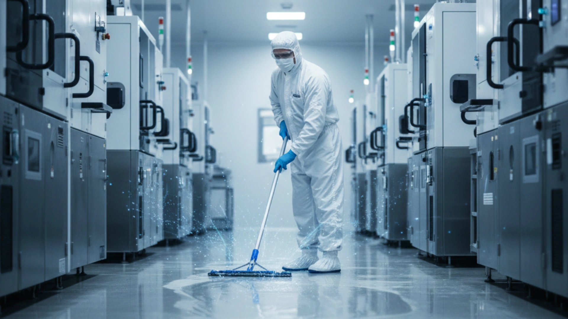
In electronics manufacturing, the mechanical action of mopping creates friction, which can generate triboelectric charges. In a low-humidity cleanroom, these charges can build up on surfaces or the operator, leading to a sudden ESD event.
Standard cleaning tools often act as insulators. When an insulator is rubbed against a cleanroom floor, it creates static that cannot be bled off to the ground. This static attracts airborne particles (“magnet effect”) and risks discharging into sensitive components.
For facilities operating under strict ESD protocols, mops should be selected as part of the site’s ESD Control Program: dissipative handles, low-charging heads, and repeatable procedures. This aligns with environments typically mapped to クラス100/1000.

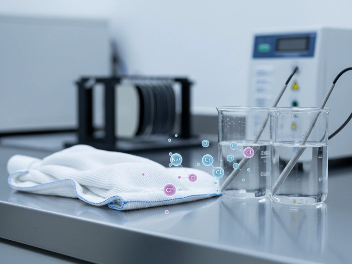
Ionic contaminants—such as sodium, potassium, chloride, and sulfate—can drive leakage, corrosion, and long-term reliability drift. In advanced nodes, “clean” must also mean イオンクリーン.
A mop may be low-linting but still heavily contaminated with ions from its manufacturing process. If the mop material was processed with hard water or contains chemical binders, ions can be deposited during mopping and later become airborne or tracked into critical process zones.
高性能 ISOクリーンルームモップ may undergo controlled laundering using high-purity DI water to reduce ionic residues and surfactants, followed by clean drying and vacuum sealing.
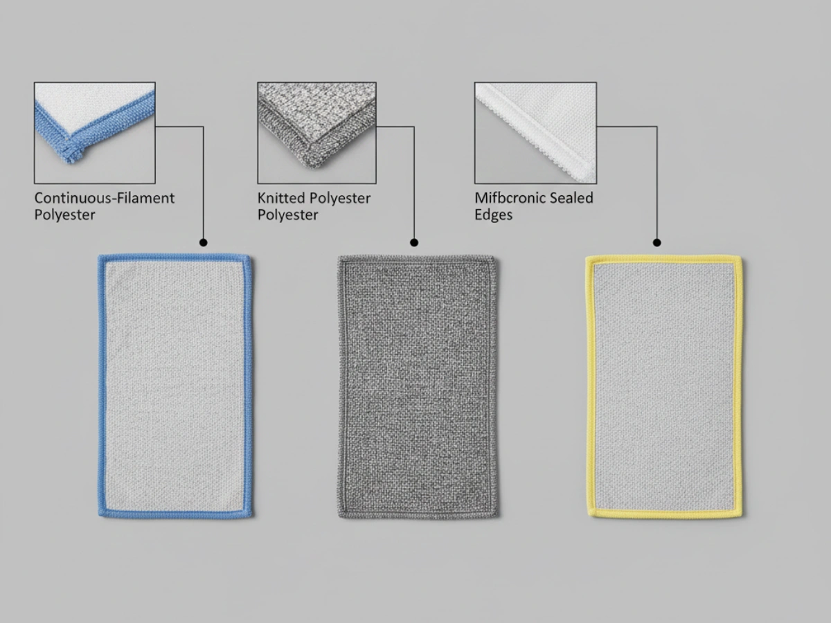
The stringency of the environment dictates the construction of the mop head. Semiconductor zones require materials that exhibit ultra-low shedding and sealed edges to prevent fiber release into airflow.
| ISOクラス | 同等 | 好ましいモップ構造 |
|---|---|---|
| ISO 3 ~ 4 | クラス 1 ~ 10 | 100% 連続フィラメントポリエステル、洗濯済み、超音波エッジ |
| ISO 5 ~ 6 | クラス 100 ~ 1000 | ニットポリエステルまたは高密度マイクロファイバー |
| ISO7 | クラス10,000 | ポリセルロース不織布またはマイクロファイバーブレンド |
最もデリケートなゾーンについては、 超音波またはレーザーシールされたエッジ help reduce loose fibers. For broader mapping across standards, see our クリーンルームモップ選定ガイド.
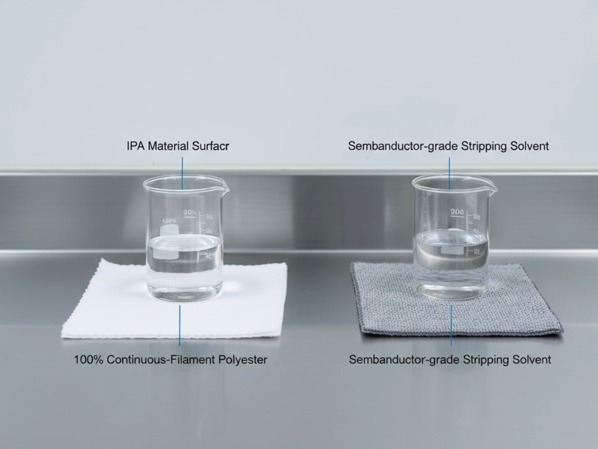
Semiconductor cleanrooms use high-purity IPA and specialized agents. Mop heads must remain chemically inert to avoid breaking down during use—and to minimize non-volatile residues (NVR).
Contamination control in electronics is a holistic discipline. Mop selection should be documented in SOPs and reviewed during yield loss investigations—especially when ESD, ionics, or particulate excursions correlate with floor control.
業界を超えた選択ロジックについては、弊社の クリーンルームモップ選定ガイド.