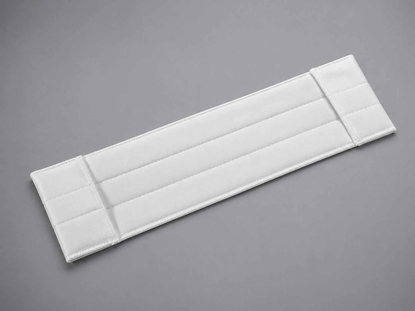
半導体のクリーンルームのモップ掛けは、医薬品のクリーンルームのモップ掛けの延長ではありません。これは、静電気放電 (ESD) の安全性、ISO クラス 3 ~ 5 の 0.1 ミクロン未満の粒子制限、および攻撃的なプロセス溶媒 (IPA、アセトン、HMDS) との適合性という、製薬およびバイオテクノロジーの文脈では存在しないか優先順位が低い 3 つの制約を同時に課します。 ISO 7 医薬品充填スイートで適切に機能するモップは、ウェーハを破壊する静電気放電を引き起こしたり、ISO 4 フォトリソグラフィー ベイの浮遊粒子バジェットを超えたり、エッチング領域で繰り返しアセトンにさらされると劣化したりする可能性があります。このガイドでは、構造化された選択フレームワーク、ゾーンごとの要件、業界間の仕様比較、半導体施設および調達チームが必要とする 8 項目の購入者チェックリストを提供します。
If a procurement team sources cleanroom mops using the same specification they apply to a pharmaceutical facility, they will almost certainly introduce a contamination or product-damage risk into their semiconductor cleanroom. The reason is not that one industry is more demanding than the other — it is that the demands are qualitatively different. Pharmaceutical cleanroom contamination control is organized around viable particulates (microorganisms), disinfectant efficacy, and sterility assurance. Semiconductor contamination control is organized around non-viable particulates, electrostatic charge, and chemical process integrity. The mop specification must reflect this difference at every parameter.
Semiconductor cleanroom mopping differs from pharmaceutical cleanroom mopping in three fundamental dimensions: (1) ESD control requirements that are either absent or optional in pharma; (2) particle size sensitivity down to 0.1 micron at ISO Class 3-5, which is 2 to 4 orders of magnitude stricter than the ISO 7-8 range typical in pharma; and (3) aggressive solvent exposure (IPA, acetone, HMDS, specialty strippers) that pharmaceutical-grade mop materials may not have been validated against. A mop specification that addresses any two of these three dimensions while neglecting the third is not suitable for semiconductor cleanroom use.
| Requirement Dimension | 製薬クリーンルーム | Semiconductor Cleanroom | モップ仕様の意味 |
|---|---|---|---|
| ESD Safety | Not typically required; ESD is rarely a consumable specification parameter | Required in all wafer-handling zones; surface resistivity typically below 109 Ω/square | Mop material must incorporate static-dissipative or conductive properties. Standard polyester knit alone is typically insulative and may not meet ESD criteria. |
| Airborne Particle Budget | ISO 7: 352,000 particles/m3 (≥0.5 μm); ISO 8: 3,520,000 particles/m3 (≥0.5 μm) | ISO 4: 352 particles/m3 (≥0.5 μm); ISO 3: 35 particles/m3 (≥0.5 μm). Particle counting begins at 0.1 μm. | Particle shedding limits are 1,000-100,000x stricter. Continuous filament construction and verified edge sealing become operational requirements, not recommendations. |
| Chemical Exposure | Disinfectants: quaternary ammonium, hydrogen peroxide, peracetic acid, sodium hypochlorite | Aggressive solvents: IPA, acetone, HMDS, Piranha solution, specialty photoresist strippers | Pharma-validated mop materials may not have been tested against solvents. Chemical degradation of mop fabric can become a hidden particle source that environmental monitoring may not directly attribute to the mop. |
| 一次汚染懸念 | Viable particulates (microorganisms) + non-viable particulates. Sterility is often the dominant parameter. | Non-viable particulates are the dominant concern. Even sub-visible particles can cause wafer pattern defects, shorts, or opens. | Particle shedding testing (Helmke drum or equivalent) at the target ISO class resolution is non-negotiable. A “suitable for cleanroom use” claim without particle bin data is not evidence. |
In a semiconductor wafer fabrication facility, the particle that matters most is invisible. At the 3 nm or 5 nm process node, a particle larger than half the critical dimension can cause a killer defect — a particle of 1.5 nm can destroy a transistor structure. Cleanroom classifications for semiconductor fabs reflect this sensitivity: ISO Class 3 permits only 1,000 particles per cubic meter at sizes ≥0.1 μm, and ISO Class 4 permits 10,000 at ≥0.1 μm. By contrast, ISO Class 7 — common in pharmaceutical sterile manufacturing — permits 352,000 particles at ≥0.5 μm, and particle counting for 0.1 μm is not even required at ISO 7.
The mop implication is direct: every contact between the mop head and the cleanroom floor or surface releases particles. A mop that generates 10,000 particles per square meter during use may be acceptable in an ISO 7 environment where the airborne particle budget is large. In an ISO 4 photolithography bay, the same mop can consume a measurable fraction of the facility’s total particle budget per cleaning event. Selection must begin with the facility’s strictest ISO classification, not with the average classification across all zones.
静電気の放電は、古典的な意味での汚染問題ではなく、製品に損傷を与えるメカニズムです。人間のオペレーターには感知できない数百ボルトの静電気により、オングストローム単位で測定されるゲート酸化層が破壊される可能性があります。モップは、表面と繰り返し高摩擦接触するクリーンルーム内で最も大きな移動物体の 1 つです。モップ掛けによって発生する摩擦帯電(カーペットの上で靴が擦れるときに静電気が発生するのと同じメカニズム)は、モップのヘッド、フレーム、ハンドルに蓄積し、近くのウェーハまたはウェーハキャリアに放電する可能性があります。
Pharmaceutical cleanrooms rarely specify ESD requirements for cleaning tools because the product (drug product, biologic) is not sensitive to electrostatic discharge in the same way. Semiconductor fabs must. Every consumable entering an ESD-protected area (EPA) must be classified by its surface resistivity, and cleaning tools are no exception. The mop specification must address not only the mop head material but the entire assembly — frame, handle, and any attachment hardware — because a single conductive path in an otherwise ESD-safe tool creates an uncontrolled discharge route.
Pharmaceutical cleanroom disinfectants — quaternary ammonium compounds, hydrogen peroxide, peracetic acid, sodium hypochlorite — are chemically aggressive in their own right, but they are predictable. Manufacturers of cleanroom consumables routinely test against standard disinfectant panels. Semiconductor process solvents — isopropyl alcohol (used for surface dehydration and general cleaning), acetone (used for photoresist stripping), HMDS (used for wafer surface priming), and specialty organic strippers — represent a different chemical challenge. These solvents can extract plasticizers, swell synthetic fibers, dissolve polymer coatings, and degrade adhesive bonds in mop construction — effects that pharma-focused mop validation programs may not cover.
The implication for procurement is straightforward: a mop supplier’s claim of “chemical resistance” is meaningless without specifying which chemicals, at what concentration, for what contact duration, and with what measured effect. Solvent-specific compatibility data must be part of the supplier evaluation. If it is not available, the facility must either conduct its own compatibility assessment or exclude the supplier from consideration for zones where solvent exposure is expected.
ESD-safe mop material selection begins with understanding the surface resistivity classifications defined by industry standards. ANSI/ESD S20.20 and IEC 61340-5-1 establish the framework for classifying materials in ESD-protected areas, and cleanroom mops fall within this framework as moving, friction-generating consumables.
| 分類 | Surface Resistivity Range (Ω/square) | Charge Behavior | Relevance to Cleanroom Mop |
|---|---|---|---|
| Conductive | < 104 | Charge flows freely — rapid discharge path | Rarely required for mop heads. More relevant for work surfaces and flooring. A conductive mop head in an EPA without a controlled grounding path can create a hazardous discharge scenario. |
| Static Dissipative (Low Range) | 104 – 107 | Charge dissipates in a controlled, moderate-speed manner | Suitable for ISO 3-4 photolithography areas where both particle control and ESD sensitivity are extreme. May require specialized conductive fiber integration. |
| Static Dissipative (High Range) | 107 – 109 | Charge dissipates in a controlled, slower manner | Most common requirement for semiconductor cleanroom mop consumables. Achievable through carbon-thread integration or static-dissipative surface treatment of polyester fabric. |
| Anti-Static (Low Charging) | 109 – 1011 | Resists triboelectric charge generation but does not dissipate quickly | May be acceptable for ISO 6-7 packaging/back-end areas where the ESD sensitivity is lower and the primary concern is charge generation during mopping rather than existing charge dissipation. |
| Insulative | > 1011 | Charge accumulates; no controlled dissipation path | Generally not suitable for any ESD-sensitive zone. Standard 100% polyester knit and untreated microfiber typically fall into this range. These materials are common in pharmaceutical cleanrooms but should not be deployed in semiconductor EPAs without verification or treatment. |
There are two primary approaches to making cleanroom mop materials ESD-safe:
The choice between these approaches depends on the facility’s mop usage model (disposable vs reusable), the target resistivity range, and the zone’s chemical exposure profile. For disposable mops in ISO 3-4 photolithography, either approach may be suitable provided the resistivity data is verified. For reusable mops with aggressive solvent exposure, carbon-thread integration typically provides more consistent long-term ESD performance than surface treatments. For a broader discussion of semiconductor-specific mop products, see semiconductor cleanroom mop products.
ESD safety is a system property, not a component property. A mop head with surface resistivity of 108 Ω/square provides no ESD protection if the operator’s garments, the cleanroom flooring, and the mop frame/handle assembly do not complete a controlled dissipation path to ground. The mop is one link in the grounding chain:
Facilities should verify ESD compatibility for the complete assembly — mop head, frame, handle, operator PPE, and flooring — rather than specifying ESD requirements for the mop head in isolation. A cleanroom mop that meets ESD resistivity specifications in a laboratory measurement may not function as an ESD-safe tool in the actual cleanroom if the assembly-level dissipation path is incomplete.
Particle generation from a cleanroom mop is not a pass/fail property — it is a quantitative measurement that must be evaluated against the airborne particle budget of the target ISO class. A mop that generates 5,000 particles per minute in a Helmke drum may be an excellent performer for ISO 7 but unacceptable for ISO 4, where the total permissible ≥0.5 μm particle count is only 352 per cubic meter. The mop specification must match the strictest zone in which the mop will be used.
The fundamental material choice affecting particle generation is fiber construction:
| ファイバーの種類 | 工事 | Particle Generation Mechanism | Typical Suitability |
|---|---|---|---|
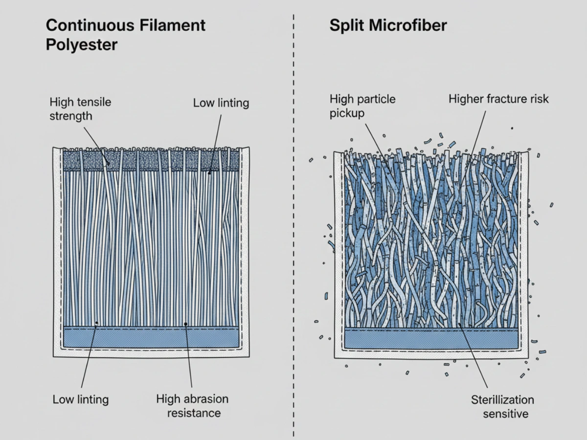
| 連続長繊維ポリエステル | Long, unbroken filaments run the full length of the yarn. No fiber ends within the fabric structure except at cut edges. | Particles are primarily generated at cut edges (which must be sealed) and from surface abrasion. Fiber-end shedding in the fabric body is inherently low because there are no staple fiber ends to break free. | Strongly preferred for ISO 3-5 semiconductor zones. The inherently lower particle shedding profile makes continuous filament the default starting point for sub-ISO-5 mop selection. |
| Non-Continuous / Staple Fiber Polyester | Short staple fibers (typically 25-50 mm) are spun together to form yarn. Thousands of fiber ends exist within the fabric structure. | Individual staple fibers can separate from the yarn during mechanical agitation (mopping). Each fiber end is a potential particle that can shed. The particle count from staple fiber constructions is generally higher than continuous filament for the same test conditions. | May be evaluated for ISO 6-7 zones. Generally not recommended for ISO 3-5 without Helmke drum data demonstrating acceptable particle shedding at the target particle size and class. |
| Microfiber (Split Polyester/Polyamide) | Bi-component fibers are split into micro-denier filaments (typically <1 denier per filament). The split structure creates high surface area for particle capture. | The same high surface area that gives microfiber its particle-capture efficiency also creates more surface from which particles can shed. The split-fiber tips are potential particle sources. The polyamide (nylon) component adds a second material with its own particle shedding and chemical compatibility characteristics. | May be evaluated for ISO 5-7 semiconductor zones. Requires more rigorous particle shedding verification for ISO 3-4 than continuous filament polyester. The cleaning efficacy/particle shedding trade-off should be assessed zone by zone. |
The body image below illustrates the continuous filament polyester fiber structure — the smooth, lint-free surface without loose staple fiber ends that makes this construction preferable for low-particle-generation cleanroom mop heads in semiconductor environments.
For a side-by-side evaluation of microfiber and polyester in cleanroom applications, see the マイクロファイバーとポリエステルのクリーンルームモップの比較.
Regardless of whether the fabric is continuous filament or non-continuous, the cut edges are the most concentrated particle source on any cleanroom mop head. When fabric is cut, filaments are severed, creating fiber ends that can release particles with every mechanical agitation. The quality of edge sealing determines how effectively these cut-edge particles are contained:
Procurement teams should request information on the edge sealing method and verify that all four edges of the mop head are sealed — not just the visible edges. For a deeper understanding of how lint generation relates to mop construction, see what is a low-lint cleanroom mop.
The Helmke drum test (per IEST-RP-CC004.3 or equivalent) is the standard method for quantifying particle shedding from cleanroom consumables under mechanical agitation. For semiconductor-grade mop evaluation, the following test parameters and expectations apply:
Critical distinction: ISO 14644 classifies environments, not products. A supplier claiming a mop is “ISO Class 5 compatible” without providing the test method, particle size bins, measured values, and test conditions is making an unverifiable claim. Facility teams should treat such claims as marketing language, not technical evidence, until test data is provided.
The chemical environment in a semiconductor fab introduces mop material compatibility challenges that pharmaceutical cleanroom mop selection guides do not address. A cleanroom mop material that withstands repeated exposure to quaternary ammonium disinfectants may degrade rapidly when contacted by acetone. The procurement process must verify compatibility against the facility’s specific chemical panel — not against a generic “chemical resistant” claim.
Isopropyl alcohol (IPA) at 70-99% concentration is the most common cleaning solvent in semiconductor cleanrooms. It is used for surface dehydration, general wipe-down, and removal of organic residues. While IPA is less aggressive than acetone or HMDS, it is a penetrant that can extract plasticizers from polymer materials, swell certain synthetic fibers, and degrade adhesive bonds used in mop construction.
For polyester-based mop materials, IPA compatibility is generally good — polyester (PET) has inherent resistance to alcohol-based solvents. However, the following elements require verification:
Acetone is used in semiconductor fabs for photoresist removal, equipment cleaning, and general degreasing. It is a strong organic solvent that attacks a wider range of polymers than IPA:
| Chemical Agent | Common Semiconductor Use | Compatibility with Mop Materials | Verification Required |
|---|---|---|---|
| IPA (70-99%) | General surface cleaning, dehydration, pre-wipe for process equipment | Polyester: Generally good. Polyamide: Fair to poor — swelling possible. ESD treatments: May degrade. | Post-exposure particle shedding assessment. ESD resistivity re-measurement after IPA contact for reusable mops. |
| Acetone | Photoresist stripping, heavy organic residue removal, equipment degreasing | Polyester: May tolerate brief contact; extended exposure can cause swelling and tensile strength loss. Polyamide: Poor — significant degradation expected. Adhesives: Most standard adhesives fail under acetone exposure. | Extended contact immersion test. Weight change, tensile strength change, and visual inspection for material degradation after acetone exposure at facility-relevant concentration and duration. |
| HMDS | Wafer surface priming for photoresist adhesion | Reacts with moisture. May not directly attack mop materials but can deposit residues that alter subsequent cleaning performance. | Residue analysis after simulated contact. Mop material surface characterization after HMDS exposure. |
| Piranha Solution (H2SO4 + H2○2) | Aggressive equipment cleaning, organic residue removal | Highly oxidative — attacks most organic polymers including polyester. Mop contact with Piranha solution should generally be avoided unless the mop material has been specifically validated for this exposure. | If mop contact with Piranha is unavoidable, request material-specific compatibility data at the facility’s exact concentration and temperature. Most standard cleanroom mop materials will degrade under Piranha exposure. |
Chemical degradation of mop materials is a contamination risk that environmental monitoring programs may not directly attribute to the mop because the effect is gradual and cumulative. The mechanism works as follows:
This degradation chain highlights why solvent-specific compatibility data is not a nice-to-have but an operational requirement. A mop material that degrades under the facility’s chemical exposure profile generates contamination that is difficult to isolate, diagnose, and eliminate after the fact.
Specifying one cleanroom mop for an entire semiconductor fab is a procurement simplification that creates contamination risk. Different fab zones have different ISO classifications, different ESD sensitivity levels, different chemical exposure profiles, and different cleaning frequencies. The mop specification should reflect the requirements of each zone — or, if a single specification is used for procurement efficiency, it should be validated against the strictest zone’s requirements, with the understanding that this may result in over-specification for less demanding zones.
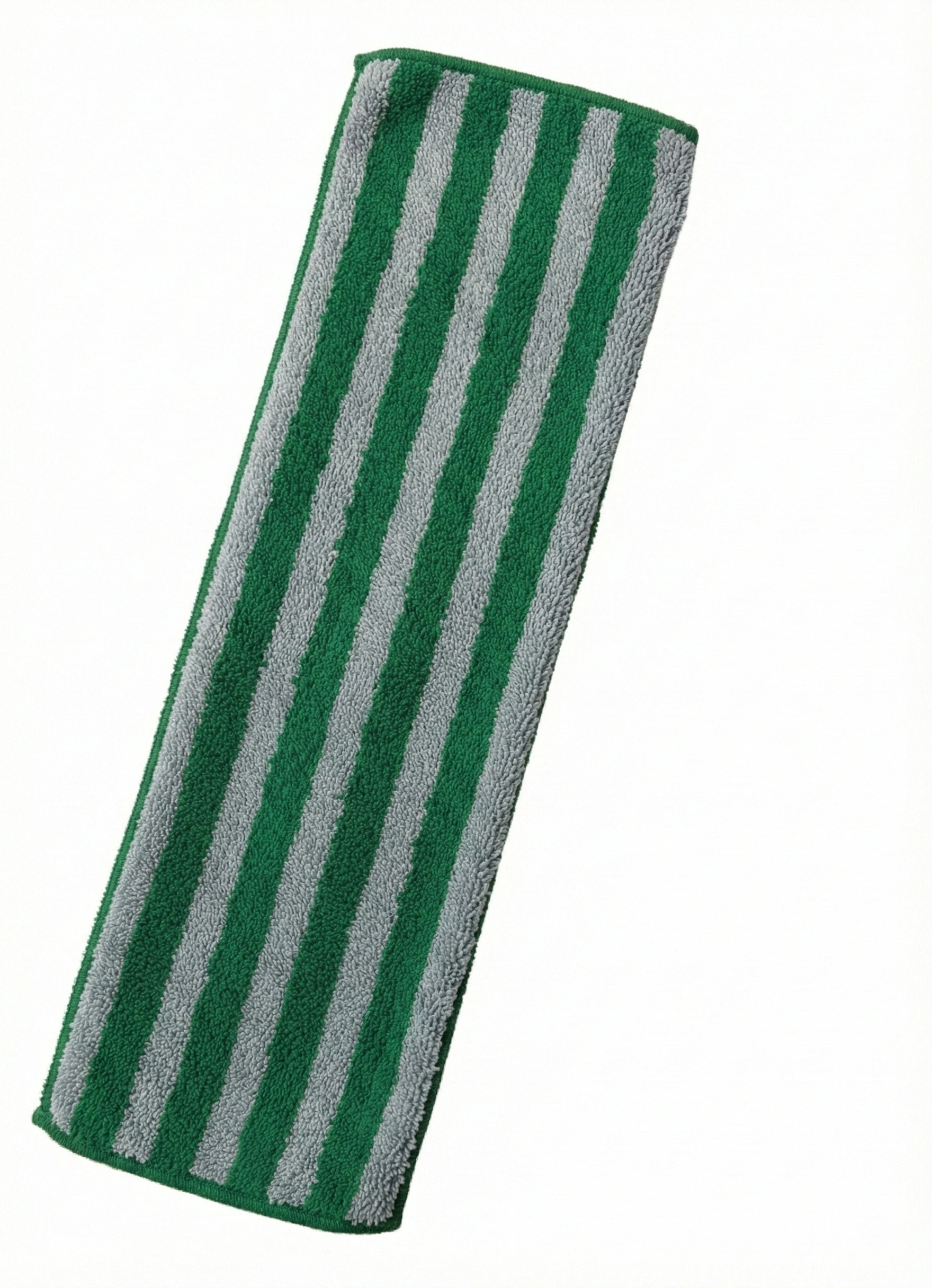
The complete mop system assembly — mop head, stainless steel frame, and telescoping handle — is shown below as an integrated cleaning platform suitable for semiconductor and electronics cleanroom environments where system-level compatibility is essential to contamination control.
Photolithography bays represent the intersection of the strictest particle limits and the highest ESD sensitivity in any semiconductor fab. The particle generated during mopping in a photolithography area can deposit on a photomask or wafer surface, creating a pattern defect that renders the wafer unusable. The photomask itself is a single-point-of-failure component — a particle defect on a mask is replicated across every wafer exposed through that mask.
Mop specification for photolithography:
Etch and chemical mechanical polishing (CMP) areas combine moderate particle sensitivity with the most aggressive chemical environment in the fab. Etch processes use strong acids and bases that can spill or aerosolize onto floors and equipment surfaces. CMP slurry contains abrasive particles that, combined with cleaning chemicals, create a chemically and mechanically aggressive cleaning environment.
Mop specification for etch/CMP:
Metrology areas house measurement and inspection equipment — scanning electron microscopes (SEM), atomic force microscopes (AFM), optical inspection tools — where a single airborne particle can interfere with measurement accuracy. The particle limits are as strict as photolithography, but ESD requirements may be equipment-specific rather than zone-wide.
Mop specification for metrology:
Packaging and back-end assembly areas operate at less strict particle classifications but handle finished or near-finished devices where ESD damage is a yield-impacting event. Throughput is higher than in front-end zones — cleaning frequency may be higher, and the mop consumable consumption rate is correspondingly higher.
Mop specification for packaging/assembly:
For further guidance on semiconductor facility-specific cleaning requirements, see the cleanroom mop for semiconductor facility ページ。
The difference between a credible cleanroom mop supplier and one making unverifiable claims is documentation. Semiconductor procurement teams should request the following documentation as part of the supplier evaluation process. Each item should be supported by test data, not verbal assurance or marketing statements.
Outgassing — the release of volatile compounds from materials under vacuum or elevated temperature — is a semiconductor-specific concern that is rarely relevant in pharmaceutical cleanrooms. In vacuum process chambers, outgassed compounds from consumable materials can deposit on optical surfaces, wafer handlers, and process equipment, creating a contamination layer that affects process consistency.
ASTM E595 is the standard test method for outgassing, measuring two parameters:
If the cleanroom mop will be used in or near vacuum process equipment, outgassing data is a required specification item. If the mop is used only in atmospheric cleanroom areas (corridors, gowning rooms, packaging areas), outgassing is less critical but still worth requesting as evidence of the supplier’s technical documentation capability.
Request the following ESD-related documentation from the mop supplier:
The particle shedding test report should include at minimum:
If a supplier cannot provide particle shedding data at the particle size resolution relevant to the facility’s ISO class, the mop cannot be considered validated for that environment.
For each solvent or chemical the mop will contact, request:
If chemical resistance data is not available from the supplier, request material composition information (polymer type, fiber construction, any coatings or treatments) to allow the facility’s own engineering team to assess compatibility. For a general framework for evaluating mop suppliers, see the cleanroom mop buyer evaluation framework.
The table below compares cleanroom mop specification requirements across four regulated industries. The intent is not to rank industries by difficulty but to highlight where the specification emphasis differs — and why a mop specification written for one vertical cannot be assumed valid for another without verification.
| Specification Parameter | 半導体 | 医薬品 | バイオテクノロジー | 医療機器 |
|---|---|---|---|---|
| Typical ISO Class | ISO 3-5 (front-end) ISO 5-7 (back-end) | ISO 5-8 (Grade A-D under EU GMP Annex 1) | ISO 5-8; ISO 7-8 most common for production suites | ISO 7-8 most common; ISO 5-7 for implantable device assembly |
| Particle Size Sensitivity | ≥0.1 μm critical. Particle budget 100-100,000x stricter than pharma at equivalent zone size. | ≥0.5 μm is the standard measurement threshold under GMP. ≥5.0 μm for Grade A viable monitoring. | ≥0.5 μm standard threshold; ≥5.0 μm for microbial risk assessment in aseptic processing areas. | ≥0.5 μm standard threshold for most devices; ≥0.3 μm may apply to implantables in ISO 5 environments. |
| ESD Requirement | Mandatory in all wafer-handling and device-handling zones. Surface resistivity typically 107-109 Ω/square. | Not typically required. ESD is not a standard cleanroom consumable specification parameter in pharma. | Not typically required for consumables. May apply in facilities handling electronic analytical equipment. | May apply in electronics-containing device assembly (e.g., pacemakers, diagnostic equipment). Not typically required for non-electronic devices. |
| 無菌要件 | Not typically required for mops. Biological contamination is generally not a process concern in semiconductor fabs. | 必須 for Grade A/B (ISO 5) zones. Sterile presentation (gamma/EtO/autoclave) with validated packaging and aseptic transfer protocol. | 必須 for aseptic processing areas. Sterility certification per batch with Certificate of Analysis (COA). | Conditional: Required for implantable or sterile devices. Not typically required for non-sterile device assembly in ISO 7-8 environments. |
| Primary Chemical Exposure | Aggressive organic solvents: IPA, acetone, HMDS, specialty strippers, Piranha solution | Disinfectants: quaternary ammonium, hydrogen peroxide, peracetic acid, sodium hypochlorite, IPA (70%) | Disinfectants + decontamination agents: hydrogen peroxide vapor (VHP), chlorine dioxide, sporicidal agents | Disinfectants: quaternary ammonium, IPA (70%), hydrogen peroxide. Solvent exposure limited compared to semiconductor fabs. |
| Outgassing Concern | 高い — especially for mops used near vacuum process equipment. ASTM E595 data may be required. | Low — outgassing is not a standard GMP concern for cleaning consumables used at atmospheric pressure. | Low for atmospheric cleanroom operations. May be relevant for isolator/RABS environments. | Low — outgassing is not a standard quality system concern for medical device manufacturing at atmospheric pressure. |
| 期待されるドキュメント | Test data heavy: Helmke drum, surface resistivity, static decay, chemical resistance, outgassing (optional). Certifications should reference specific test methods. | コンプライアンス重視: 無菌証明書、COA、バッチトレーサビリティ、二重袋包装の検証、付録 1 の調整文書。 | 組み合わせ: 無菌認証 + 除染剤の適合性 + トレーサビリティ。バイオバーデン管理データが要求される場合があります。 | 中程度: ISO 分類互換性ステートメント、材料組成情報、無菌性が必要な場合のパッケージングの完全性。 |
| モップの材質の好み | ISO 3-5 に適した連続フィラメント ポリエステル。 ESD のための静電気消散処理またはカーボン統合。 ISO 5-7 で評価されたマイクロファイバー。 | ポリエステルニット(ゾーンに応じて連続または非連続)。 ISO 7-8 に適合するマイクロファイバー。マテリアルの選択は、パーティクルの制限に依存するよりも、ワークフローに依存します。 | Similar to pharma: polyester knit dominant. Autoclavable materials may be preferred for facilities with steam sterilization capability. | Polyester knit dominant. Mop selection is more application-driven (device type, cleaning zone, frequency) than particle-limit-driven. |
この比較から得られる重要な点は、ある業界では最も重要なパラメーター (製薬の無菌性、半導体の ESD、バイオテクノロジーの除染剤の適合性) が、別の業界では無関係または二の次である可能性があることです。医薬品の無菌製造が検証されたモップは、無菌性と消毒剤の適合性についてはテストされている可能性がありますが、ESD 表面抵抗率やアセトンの適合性についてはテストされていないことがほぼ確実です。モップの適合性に関する業界間の思い込みは、クリーンルームの消耗品調達において最も一般的な仕様ミスです。
バイオテクノロジーおよび製薬施設におけるモップ要件の集中的な比較については、以下を参照してください。 バイオテクノロジーと製薬のクリーンルームモップの違い.
Selecting a cleanroom mop for semiconductor and electronics manufacturing requires a specification process that addresses three constraints simultaneously: ESD safety, particle limits at the target ISO class, and chemical compatibility with the facility’s solvent panel. The process should be zone-specific — a photolithography bay has different requirements than a packaging area, and specifying one mop for the entire fab transfers the risk of the most demanding zone to all other zones.
The recommended procurement approach is:
A mop specification that addresses all three constraints — ESD, particles, and chemicals — and is validated with supplier documentation and in-situ testing, reduces three of the most common sources of cleanroom contamination risk in semiconductor manufacturing to a single, controlled variable.
Not typically. Semiconductor cleanroom contamination control is organized around non-viable particulates, electrostatic charge, and chemical residues — not biological contamination. Sterile mops are generally not required for standard semiconductor manufacturing operations. However, if a semiconductor facility also houses biotech or pharmaceutical operations, sterile mop requirements may apply to those specific zones. The decision should be based on the facility’s contamination control plan for each zone, not on a blanket “all cleanrooms need sterile mops” assumption. If sterile mops are specified, the sterilization method (gamma, EtO, autoclave) must be verified as compatible with any ESD treatment applied to the mop material, as some sterilization processes can alter surface resistivity.
ESD 保護が必要なほとんどの半導体クリーンルーム ゾーンでは、モップは静電気拡散率 10 の範囲内に収まる必要があります。7 to 109 Ω/平方 (表面抵抗率)。この範囲では、敏感なデバイスにとって危険となる可能性のある急速な放電経路を作成することなく、制御された電荷散逸が可能になります。 ESD 感度が最も高い ISO 3 ~ 4 のフォトリソグラフィ領域では、この範囲の下限 (107 to 108 Ω/平方)を指定できます。中程度の ESD 感度を持つ ISO 6 ~ 7 のパッケージング/バックエンド領域の場合、静電気防止範囲は 109 to 1011 既存の電荷を散逸させるのではなく、モップ掛け中の摩擦帯電の発生を防ぐことが主な関心事である場合、Ω/平方は許容される可能性があります。ターゲット範囲に関係なく、サプライヤーは測定された抵抗率データをテスト方法のリファレンスとともに提供する必要があります。測定値とテスト条件のない「ESD 安全」の主張は検証可能な仕様ではありません。
一般的にはノーです。少なくとも、製薬用モップの仕様で一般的に取り上げられていない 3 つのパラメーターについて独立した検証がなければ、そうではありません。まず、ESD の安全性です。標準的な製薬用クリーンルーム モップは通常、カーボン糸の組み込みや静電気拡散処理を施していない 100% ポリエステル ニットで作られており、絶縁範囲内にあります (>109 Ω/平方)は、半導体の ESD 要件を満たしていません。第二に、粒子制限: 医薬品モップは ISO 5 ~ 8 環境で検証されていますが、粒子放出データは通常 0.5 μm 以上であり、ISO 3 ~ 4 半導体ゾーンに関連する 0.1 μm 以上の分解能ではありません。第三に、溶剤の適合性: 医薬品モップは、有機溶剤ではなく、消毒剤に対して検証されています。半導体工場で使用される医薬品モップには、3 つの未検証の変数が導入されています。施設が半導体用途の製薬グレードのモップを評価することを選択した場合、対象ゾーンの要件に応じてこれらの各パラメーターを個別に検証する必要があります。
Microfiber mops may be evaluated for semiconductor use, but the evaluation must address three caveats specific to semiconductor environments. First, particle shedding: the split-fiber structure that gives microfiber its particle-capture advantage also creates more fiber tips and surface area from which particles can shed. This is less of a concern at ISO 5-7 but requires rigorous Helmke drum verification at ISO 3-4. Second, chemical compatibility: the polyamide (nylon) component in standard microfiber blends has lower resistance to acetone and other organic solvents than 100% polyester. Microfiber mops used in areas with solvent exposure should be verified for polyamide-specific chemical compatibility. Third, ESD treatment durability: if the microfiber has been treated for ESD properties, the treatment must be verified as durable through the expected use cycle — microfiber’s higher surface area may accelerate the degradation of topically applied ESD treatments compared to continuous filament polyester. Microfiber is more commonly deployed in ISO 5-7 semiconductor zones (packaging, back-end) than in ISO 3-4 front-end zones.
はい。 ESD の安全性はシステムの特性であり、コンポーネントの特性ではありません。ゾーンに ESD 要件がある場合は、モップ アセンブリ全体 (ヘッド、フレーム、ハンドル、および取り付けハードウェア) の ESD 準拠を評価する必要があります。よくある見落としは、導体として機能する可能性のある標準的なステンレス鋼またはアルミニウムのフレームとハンドルを使用しながら、ESD 安全なモップヘッドを指定することで、制御されない電荷散逸経路が形成されることです。アセンブリ評価では、以下を検証する必要があります。(1) モップヘッドの材質が表面抵抗率の要件を満たしていること。 (2) フレーム素材とプラスチックフレームコンポーネントは、モップヘッドとハンドルの間に絶縁障壁を形成しません。 (3) ハンドル グリップの素材は、オペレータの手袋との ESD 互換性があります。 (4) 個々のコンポーネントだけでなく、完全なアセンブリには、施設の ESD 制御計画と互換性のある、検証済みのグランドへの放散経路があります。
The mop should be validated for the strictest ISO class in which it will be used. If a semiconductor fab operates at ISO 3 in photolithography, ISO 4 in etch, and ISO 6 in packaging, the mop specification should be validated against ISO 3 particle limits — or separate mop specifications should be maintained for different zone classes. A common procurement error is validating the mop at the facility’s average ISO class rather than its strictest. An “ISO 5 mop” used in an ISO 3 photolithography bay may shed particles at a rate that, while imperceptible at ISO 5, consumes a measurable fraction of the ISO 3 airborne particle budget with each cleaning event. The safest approach is zone-specific specification — different mops for different ISO classes — which also allows cost optimization: less demanding specifications (and potentially lower-cost mops) for ISO 6-7 zones.
A verifiable ESD claim includes five elements: (1) the measured surface resistivity value in Ω/square (not a range statement like “ESD-safe” or “anti-static”); (2) the test method reference (e.g., ANSI/ESD STM11.11, IEC 61340-2-3); (3) the test conditions — temperature and relative humidity at the time of measurement — because surface resistivity is humidity-dependent and a measurement at 50% RH may differ significantly from the same material at 12% RH; (4) the scope of the measurement — mop head fabric only, or fully assembled mop including frame and handle; and (5) for reusable mops, resistivity data after the specified number of laundry cycles to demonstrate ESD treatment durability. If a supplier cannot produce a test report containing these elements, the ESD claim should be treated as unverified. A credible supplier maintains this documentation as part of their standard technical data package.
Request material compatibility data for each solvent the mop will contact during use — do not accept a general “chemical resistant” statement. For each solvent, the test data should specify: the chemical agent and concentration tested, the test method (immersion, droplet exposure, or wipe contact), the contact duration, and the measured effects — minimum weight change (%), visual inspection for swelling/delamination/color change, and ideally tensile strength change (%). Post-exposure particle shedding data is valuable: does the mop generate more particles after chemical exposure than before? If the supplier does not have solvent-specific compatibility data, request the complete material composition (polymer types, fiber construction, any coatings, adhesives, or treatments) so the facility’s engineering team can assess compatibility. The most common gap in semiconductor mop procurement is assuming that pharmaceutical disinfectant compatibility data extends to organic solvent compatibility — it generally does not.
Share your target ISO class, ESD resistivity requirements, and solvent cleaning panel with MIDPOSI. Our team will help assess whether the White Cleanroom Mop Series meets your facility’s semiconductor-grade specifications for particle control, electrostatic discharge safety, and chemical compatibility — with documentation support for your supplier qualification process.
White Cleanroom Mop Series — continuous filament polyester construction — 40g, 55g, 65g configurations — sterile and non-sterile options — particle shedding data and material specifications available upon request for semiconductor facility evaluation